PCB design rule (DRC) checklist
A design-rule checklist for PCB release: clearance, annular ring, drill-to-copper, silkscreen and vias, based on IPC-2221 and common fab notes.
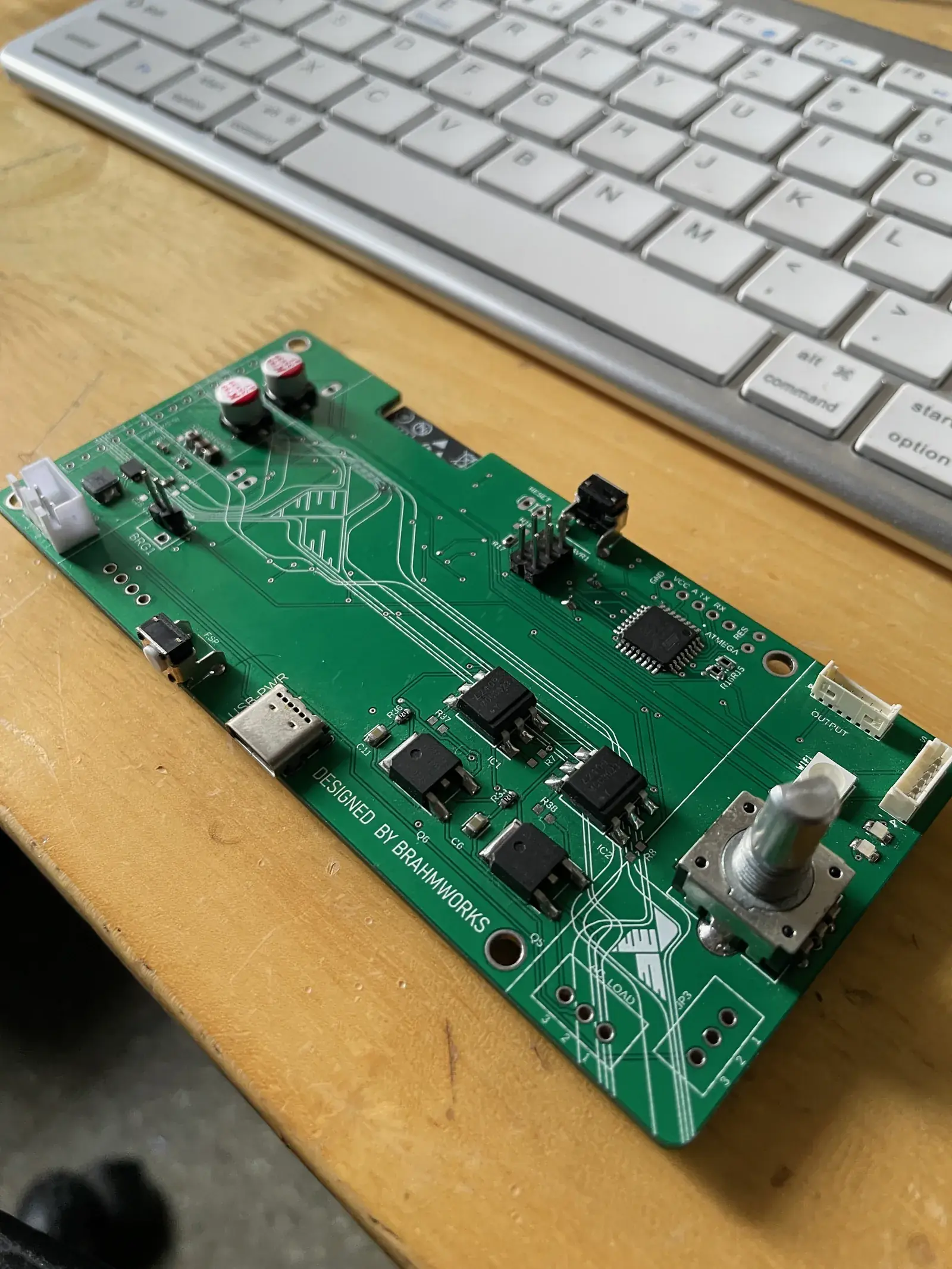
Software DRC will not save a board if the rules you loaded are wrong, or if the problem is not a spacing error — a via in a pad you cannot fill, a silkscreen over a landing, a high-voltage gap that meets the CAD rule and fails IPC-2221 Table 6-1. This checklist is a category-by-category walk before you send Gerbers: clearance, annular ring, drill-to-copper, silkscreen, and via practice, written against IPC-2221 and against what fab houses commonly ask for.
A few numbers are worth memorising as starting points, then confirming with your fab and your class (IPC-6012 Class 2 is a typical commercial default; Class 3 is tighter). Annular ring is (pad diameter − drill) / 2; a commonly cited Class 2 minimum is about 0.125 mm, and drill wander makes that a real limit, not a theoretical one. High-voltage clearance is not the same as your 0.15 mm fabrication clearance: at 250 V AC, IPC-2221 has a much larger external clearance (often cited around 1.6 mm — always check the table for the voltage and the coating).
The list also covers ordinary release hygiene: soldermask expansion, courtyard collisions, fiducials, tool-hole sizes the fab can actually drill, and whether unplated holes are specified as such. Your CAD rule file should be updated to match the fab you will use, then this list used as a human pass for the things rules do not express well.
Run the checklist on the finished board, not only on a default template. A last-minute connector move is how annular rings and courtyard errors appear.
Example
A near-miss the list is there to catch. A 0.5 mm drill in a 0.7 mm pad looks like a pad in CAD and leaves only 0.1 mm of annular ring before tolerance — below a typical Class 2 target once the drill walks. Enlarging the pad, shrinking the drill if the current and the fab allow, or moving the via are all better than hoping the first article plates correctly. Check the ring on every via, not only on the ones you stared at.
How to use this tool
- Load or write a rule set that matches your fab’s capabilities and the IPC class on the purchase order.
- Run the CAD DRC and fix every real error; do not disable a rule to get a green tick.
- Walk this checklist for annular ring, high-voltage gaps, silkscreen, and mechanical holes.
- Confirm the stackup, copper weight and finish in the fab notes match the design.
- Export Gerbers or ODB++ and, if you can, review a CAM plot before you pay for the run.
Frequently asked questions
Does this replace my CAD’s DRC?
No. It sits on top. CAD DRC is necessary and not sufficient. The checklist is for class rules, voltage, and release items a default rule file often misses.
What annular ring should I use?
Follow the IPC class and the fab. A commonly used Class 2 starting point is a 0.125 mm minimum finished annular ring, with pads large enough to survive drill tolerance. Class 3 is tighter. Ask the fab if you are close to the limit.
Where do voltage clearances come from?
IPC-2221 Table 6-1 (and related standards such as IPC-2221A and, for some products, IEC spacing rules) is the usual reference. CAD clearance is often set to a fabrication minimum and will not automatically become a mains-rated gap.
When should I use filled and capped vias?
When you have vias in pads, fine BGA escape, or a reliability need your fab supports. It is a process option with a cost, not a default for every via.